
As feature sizes on substrates and masks/reticles continue to shrink, the tolerance for defects in both starting materials and finished devices continues to decrease. Not only are we approaching zero tolerance for known defect types (particles, crystal defects, etc.), but as manufacturing moves into the deep nanoscale, manufacturers continue to discover equipment susceptibility to entirely new types of defects. Furthermore, available metrics for defect detection need to sense and quantify defects at noise levels very close to their operating principles, and new defect detection methods are constantly being developed.
Scanning Defect Inspection
Before production begins, bare wafers are qualified at the wafer manufacturer and again when they are received at the semiconductor fab. These qualification processes locate, map, and differentiate between pre-existing defects and those that arise during the IC manufacturing process. Only wafers with the fewest defects are used in production, and pre-production defect maps allow manufacturers to track areas that may cause bad chips. Bare or unpatterned wafers are also measured before and after passing through passive or active process environments to establish a baseline for particle contributions from a specific process tool.
Topography Inspection
There are many reasons why bare wafer topography needs to be measured. For example, the wafer may bend, or the chuck (electrostatic or pneumatic) holding the wafer may create indentations at the contact points with the wafer. This deformation affects the imaging of patterns at the nanometer scale. Extremely precise interferometry stages have been developed to measure changes in wafer shape before the process begins.
Differential Image Inspection
Optical inspection of patterned wafers can use brightfield illumination, darkfield illumination, or a combination of both for defect detection.
Customized optical solutions for wafer inspection
We provide optical subsystem design and manufacturing solutions for wafer inspection machine manufacturers. Many manufacturers at home and abroad choose CNI light sources for semiconductor inspection.
Laser Related
261nm & 320nm Parameters:
| Wavelength (nm) | 261±1 | 320±1 |
| Operating mode | CW | |
| Output power (mW) | 1-1000 | 1-3000 |
| Power stability (rms, over 4 hours) | <3%, <2%, <1% | |
| Transverse mode | Near TEM00 | |
| Beam diameter at the aperture (1/e2, mm) | <3.0 | |
| Beam divergence, full angle (mrad) | <3 | <5 |
| Polarization Ratio | >50:1,Vertical (Horizontal Optional) | |
| Warm-up time (minutes) | <10 | |
| Cooled method | Fan Cooled / Water Cooled | |
| Operating Temperature (°C) | 10-35 | |
| Power supply | 90-264VAC or 12V DC | |
| Warranty | 1 year | |
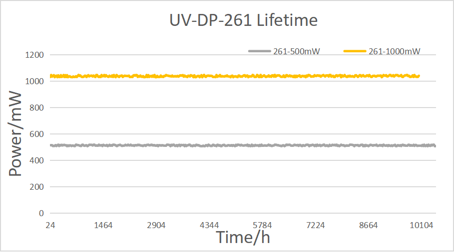
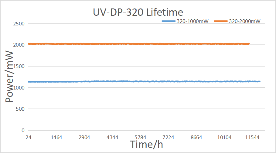
Lifetime Data
 |
 |
Other Data
 |
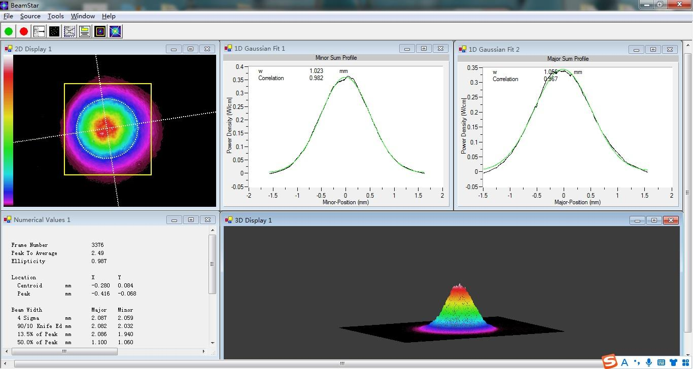 |
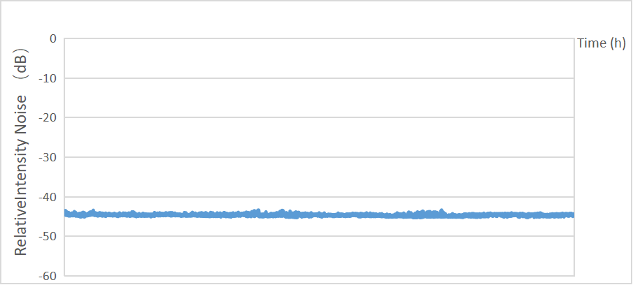
| 320nm laser noise test | Beam quality test |


